



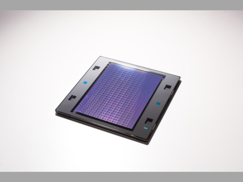
Dai Nippon Printing Co. Ltd., has successfully achieved the fine pattern resolution required for photomasks for logic semiconductors of the beyond 2nm (nm: 10-9meter) generation that support Extreme Ultra-Violet (EUV) lithography, a cutting-edge process in semiconductor manufacturing.
DNP has also completed the criteria evaluation for photomasks compatible with High-Numerical Aperture, the application being considered for next-generation semiconductors beyond the 2nm generation, and has commenced the supply of evaluation photomasks. High-NA EUV lithography makes it possible to form fine patterns on silicon wafers with a higher resolution than previously possible, and is expected to lead to the realization of high-performance, low-power semiconductors.

Development
- To realize photomasks for beyond 2nm generation EUV lithography, requires patterns 20% smaller than those for the 3nm generation. This refers not only to the size and shape of the patterns, and technology required to resolve fine patterns of all types on the face of the same mask. This includes not only standard straight and rectangular patterns but also increasingly complex curved patterns. DNP has achieved the pattern resolution required for the beyond 2nm generation by making repeated improvements based on the established 3nm generation manufacturing process.
- Photomasks for high NA-EUV lithography require higher precision and finer processing than those for standard EUV lithography. DNP established and optimized a manufacturing process flow that differs from that for conventional EUV lithography photomasks.
Going Forward
DNP will continue to establish production technologies with the goal of commencing mass production of photomasks for 2nm generation logic semiconductors in FY 2027.
DNP will also continue to cooperate with imec to promote the development of photomask manufacturing technologies with an eye toward the 1nm generation.
1: Compliant with IRDS standards
2: Numerical Aperture (NA) is a number that indicates the brightness and resolution of an optical system. High-NA refers to the expansion of the lens NA of EUV exposure equipment from the conventional 0.33 to 0.55.